FPGAs for Software Engineers 0: The Basics
Fri, Dec 13, 2019 Companion code for this post available on GithubIn this (increasingly lengthy) post, I will attempt to cover enough of a grounding in what an FPGA is and how it is configured that others out there can start to play around with writing HDL of their own. Be warned that I am by no means an expert on FPGAs, and so information here is only correct to the best of my own knowledge! There is no required hardware to follow along with this post. All tools are open source. I will assume some familiarity with C build tools.
What is an FPGA?
An FPGA (Field Programmable Gate Array) is, first and foremost, NOT A CPU (out of the box, at least). Rather than being a fixed silicon implementation that can only execute what it was made for (like a 74 series logic chip, or an Intel CPU, or an ARM based microcontroller), an FPGA is a large array of basic building blocks, each of which generally implements a very simple truth table. However, on their own these individual blocks would be fairly useless. In order to combine them to form more complex logic, FPGAs also contain a dense set of programmable connections between these logic elements, generally referred to as the routing fabric. If you envision each logic element as a single chip, the routing fabric is a set of programmable wires between all of them. FPGAs can have between hundreds and hundreds of thousands of these individual logic elements, and it is through the combination of many of these blocks that complex logic like conventional CPUs and dedicated special-purpose computation engines can be constructed.
Let’s take a look at a current FPGA, the Lattice ECP5. The figure below is taken from the Lattice ECP5 family datasheet, and shows the Programmable Functional Unit, one of the lower level blocks that make up the FPGA fabric.
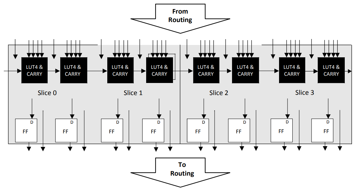
ECP5 Programmable Functional Unit (PFU) block
We can see here the two main building blocks within an FPGA - the LUT (Look Up Table) and the Flip Flop (FF). In this case, we have a LUT4 - a lookup table with 4 inputs. With one LUT4, you have 2⁴ = 16 possible states that you can encode. This means that you can trivially perform calculations like AND, OR, XOR, NOT (with up to 4 1-bit inputs) with a single LUT by loading in the appropriate truth table. You are of course not limited to those common boolean operations - a LUT can implement any truth table you may want to create. If it helps to think about FPGAs as compared to discrete logic ICs, an FPGA is essentially hundreds of thousands of individual 74xx logic chips, waiting to be connected together. Thus, anything you could create by hand with discrete logic can also be represented inside the FPGA, without having to breadboard and jumper wire each individual logic element by hand. The other core primitive here is the Flip-Flop, usually of the D variety. These are necessary for buffering outputs of combinatorial logic (LUTs), or as storage for small data (e.g. registers) that you may use in your design.
In addition to the LUT and FF basic elements, many FPGAs also contain some amount of random access memory (RAM), usually of 2-3 distinct classes:
- Block RAM: Large contiguous blocks of dedicated SRAM. There are a fixed number of these available in a given FPGA, with individual sizes usually ranging from 8KiB to 32KiB. They generally support various access widths.
- Distributed RAM: Generally smaller (on the order of several byte) blocks of RAM, distributed throughout the FPGA fabric. May be faster access than the block ram.
- LUT RAM: This term refers to using ordinary LUT+FF blocks as memory storage, wherein the FF stores one bit of data and the LUT contains the logic necessary for handling stores to that bit. Since this uses ordinary LUTs, the amount of LUT RAM available to you is bounded more by your tradeoff between logic requirements and data storage requirements.
Finally, FPGAs may implement some other special purpose logic elements that can be tied into your design. These include Multiply/Accumulate (MAC) elements, Digital Signal Processing (DSP) elements or full peripherals such as SPIs. These blocks can vary significantly between different FPGA families, so refer to the relevant datasheet for more details on these.
Why would you use an FPGA?
Given the wide and varied offerings of increasingly cheap microcontrollers on the market, you may wonder why you might want to use an FPGA in a project. There are after all negatives to FPGAs - they come with next to nothing built-in. If you get a new microcontroller, you already have a CPU core, peripherals (GPIO, I2C, SPI, etc.) and an interconnect bus tying it all together. With a few bytes of assembly instructions you can write some peripheral registers, and you’re good to go. With an FPGA, at first power on you have absolutely nothing. If you want a CPU, you have to buy, download or build the HDL for one from scratch. You need to implement any connections between your CPU and the peripherals (which, again, YOU have to build into the design).
However, the power of the FPGA is in the fact that you can do these things. If you have a microcontroller, and realize you need another I2C master, you need to go out and buy a different chip. If you discover that your SPI communication is experiencing clock skew, you have to feed the reflected clock back into another SPI peripheral to account for it, which might not be possible or might again require changing out your hardware. But with an FPGA, if you need a new I2C master, you just generate one. If you need to tweak the details of how your SPI master works, you just change the HDL that describes it. Add more FIFO space, clock the MISO line from a reflected CLK signal, whatever you want to change is within your power to change, provided you have the LUTs to do so. This makes FPGAs very powerful for applications where you need to do something specific and do it fast, such as
- Number crunching very wide numbers (you can build a vectorized ALU with as many bits as you have gates for)
- Performing multiple computations steps in a guaranteed real-time
- Parallel computation (If you want 16 Z80 processors, just add them)
Hardware Description Languages
What they are not
Now that we have somewhat of a handle on what an FPGA is and when we might want to use one, let’s take a look at how we actually “program” an FPGA. The first thing that I would say to anyone coming to FPGAs from a software background is that:
This is a very important thing to un-learn, otherwise you may struggle to intuitively understand what is happening in HDLs such as Verilog or VHDL. A programming language like C essentially defines a set of steps that are serial by default. For example, in this code:
int a = 3;
int b = a + 2;
return a + b;
As a programmer, you understand that we first assign 3 to a. Only after we have
finished assigning 3 to a do we calculate b, and only after that do we add it
back to a and return.
This makes sense, since the interface CPUs present to
the end user is that they run one instruction, then the next, and so on (even
if under the hood, they are speculatively executing and reordering your
instructions).
However, on an FPGA, all operations can be thought of as parallel by default. Let’s take a look at the following Verilog:
module foo(
    input wire [7:0] in_a,
    input wire [7:0] in_b,
    output wire [7:0] o_ret1,
    output wire [7:0] o_ret2);

    assign o_ret1 = in_a + in_b;
    assign o_ret2 = (in_a * 2) + in_b;

endmodule
In this module, the calculations for o_ret1 and o_ret2 happen continuously.
This is to say that whenever the input values change, the output also updates,
as fast as it is physically possible for the FPGA to do so.
Since each statement will instantiate
it’s own hardware, these two calculations will also run parallel to each other,
such that o_ret1 and o_ret2 will both update at the same time (plus or minus
variance in the propagation delay of their logic paths), rather than one after
the other.
In general, any statement in verilog that stands on its own
will be encoded as it’s own logic, and so happen in parallel with other
statements. Since what’s happening is not that your code is taking turns to
execute on a shared hardware resource (CPU), your code is defining the hardware
resources that calculate the desired results. And this points at the crux of the difference:
Hardware Description Languages define how to build a circuit.
Not internalizing this difference early on led me personally to spend a lot of time struggling to understand HDLs. Don’t make my mistake!
What they are
As stated before, Hardware Description Languages (HDLs) define circuits. In
Verilog, the two basic elements are reg and wire:
regis used to define a 1 or more bit data register (a D flip-flop). Registers are required anywhere you need to store data, either for computation on later clock cycles or as an output buffer from a module so that downstream logic can sample the data without seeing intermediate states of the next computation.wireis used to connect things together (like a real wire in the discrete chips analogy). Wires cannot store state - you must use a register for that. Wires however can encode combinatorial logic - it is valid to assign a wire to the result of a simple calculation, such as the sum of two other signals. Synthesis tools may insert registers wire definitions if it would be required for the design to work.
Groups of registers and wires can be encapsulated into Modules, which can then be used as their own primitives. This allows us to quickly build up complex behaviours from progressively smaller primitives. A single clocked flip-flop can be repeated to create a FIFO, which can be included as part of a peripheral, several of which can be connected to the same bus for a CPU to access.
What assignment means
In Verilog, there exist three assignment operators:
=: Blocking assignment. Verilog may not execute any following statements in the same always block until this assignment has been evaluated. The left hand side of the assignment will have the new value when the next statement is executed. Use for combinatorial logic.<=: Non-blocking assignment. These statements are executed in two steps by the verilog abstract machine: On the first timestep, all right-hand side values are computed, effectively in parallel. On the second timestep, all left-hand values are updated with the calculated right-hand values. Use for sequential logic.assign: Continuous assignment. Equivalent to=when used outside of analwaysblock.
Blocking assignment is primarily useful for combinatorial / unclocked logic. It allows you to write logic that looks more like a classical program - for example, the following defines a simple combinatorial logic setup:
module blocking(input wire a, input wire b, input wire c, output wire d);
    wire a_xor_b = a ^ b;
    assign d = c & a_xor_b;
endmodule
Non-blocking assignments are what make sequential logic possible, because of the two-step evaluation. The two time quanta represent the time just before and the time just after the trigger event for the block containing the logic (a positive clock edge, for example). If we consider the following simple divide by 2 oscillator design we can see why this is important:
module osc(input wire i_clk, output reg o_clk);
    always @(posedge i_clk)
        o_clk <= ~o_clk;
endmodule
If we were to use a blocking assignment here, assigning o_clk to itself
would be unresolvable!
However, with the two time-steps of the non-blocking assignment this allows
triggered logic to function properly - on the first time quanta the new value
(the inversion of o_clk) is calculated, and then only on the second is
it updated. It is then stable until the next update event.
Combinatorial Logic
Using just our knowledge of wires and assignments, let’s see if we can create a module that will add two (one-bit) numbers together, in addition to a carry-in and carry-out bit. This is known as a Full Adder.
//// A full-adder circuit with combinatorial logic
// We start by defining our new module, with the name 'full_adder'
module full_adder(
    // We have three inputs to our module, the two bits to be added
    // as well as the carry-in value.
    // By default, a wire is one bit wide.
    input wire in_a,
    input wire in_b,
    input wire in_carry,
    // We will output two things: the sum result, as well as whether
    // the sum overflowed (the carry-out).
    output wire out_sum,
    output wire out_carry
);

// The truth table for a fill adder is like so:
// A B Cin | Sum Cout
// --------|--------
// 0 0  0  |  0   0
// 1 0  0  |  1   0
// 0 1  0  |  1   0
// 1 1  0  |  0   1
// 0 0  1  |  1   0
// 1 0  1  |  0   1
// 0 1  1  |  0   1
// 1 1  1  |  1   1

// Based on the truth table, we can represent the sum as the XOR
// of all three input signals.
assign out_sum = in_a ^ in_b ^ in_carry;

// The carry bit is set if either
// - Both A and B are set
// - The Carry in is set and either A or B is set
assign out_carry = (in_a & in_b) | (in_carry & (in_a ^ in_b));

endmodule
To see what exactly this verilog will synthesize to, we can use
Yosys
to read the verilog and generate a flowchart showing each generated primitive
and the connections between them. The yosys invocation I use for this is like
so:
yosys -q << EOF
read_verilog full_adder.v; // Read in our verilog file
hierarchy -check; // Check and expand the design hierarchy
proc; opt; // Convert all processes in the design with logic, then optimize
fsm; opt;  // Extract and optimize the finite state machines in the design
show full_adder; // Generate and display a graphviz output of the full_adder module
EOF
This command on the module above should result in an output that looks a bit like this:
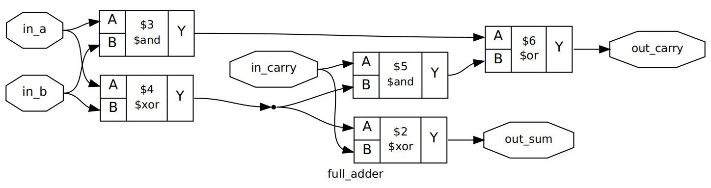
Synthesized Full Adder
The inputs/outputs of our module can be seen in the octagonal labels. From
there we can follow the connections to the lower-level blocks that yosys has
used to implement our design. If we follow the out_sum label backwards, we
can see that the in_carry value is XORed with the output of the XOR of the
in_a and in_b signals, which satisfies the wire assignment we made above in
the module definition. Similarly, we can see the logic blocks that make up the
calculation of out_carry. Notably, we have no buffers in this design - all of
these wire assignments are continuous assignments. out_carry and out_sum
will update as fast as possible when any of in_a, in_b or in_carry
change, bounded only by the propagation delay of the FPGA you might run this
on.
Sequential Logic
As with discrete electronics, one doesn’t always want a purely asynchronous setup. Adding a clock and buffers to a design allow for real hold times for data buses, and avoids potential instabilities during long calculation chains. The same is true on FPGAs - while combinatorial logic is good for small chunks of logic, it is generally the case that you will want to tie it into a sequential design for usage. As an example, let’s take the full adder we wrote above and make a 4-bit synchronous adder with it.
// Clocked adder of 4-bit numbers, with overflow signal
module adder_4b(
    // Input clock. At the positive edge of this clock, we will update the
    // value of our output data register.
    input wire i_clk,
    // Input 4-bit words to add. Syntax for multi-bit signals is
    // [num_bits-1:0] (so a 4 bit signal is [3:0]). Individual bits or
    // groups of bits an be accessed using similar notation - signal[1] is
    // the 1st it of that signal. signal[2:1] would be a two-bit slice
    // of signal.
    input wire [3:0] in_a,
    input wire [3:0] in_b,
    // Output data buffer containing the result of the addition.
    // Note that this is a reg, not a wire.
    output reg [3:0] out_sum,
    // Single output bit indicating if the addition overflowed
    output reg out_overflow
);

// Define two internal wires. We need these to connect the full adder
// elements together as a bus that we can then load into our output buffer.
wire [3:0] full_adder_sum;
wire [3:0] full_adder_carry_outs;

// We now need 4 full adders, with the carry out of each one fed into
// the carry in of the next.
// We could write out all of these by hand, but there exists a verilog
// keyword 'generate', which makes repeated declaration of elements like
// this a lot simpler.

// Because our first adder is special, we need to keep it outside the loop
full_adder adder_0(
    // Take the 0'th bit of the input words as operands
    in_a[0], in_b[0],
    // Since this is the first bit, the carry-in can be hard-coded as 0.
    1'b0,
    // The output signals can be connected into the bus we made above so
    // that they can be used by the next adder
    full_adder_sum[0],
    full_adder_carry_outs[0]
);

// Now we can generate the rest of the adders.
// First, we need to define a loop variable for the generate, like
// we would in any programming language
genvar i;
// Counting from 1 to the total number of bits in the operands, generate
// a new full adder that operates on that bit of the input words, plus
// the carry of the prevoius adder.
generate
// We use the function $bits to get the width of our in_a parameter, so
// that if it changes we don't need to modify this code.
for (i = 1; i < $bits(in_a); i++)
    full_adder adder(
        // Add the i'th bit of both operands
        in_a[i],
        in_b[i],
        // Use the carry-in from the previous adder
        full_adder_carry_outs[i-1],
        // Connect our sum output to the full adder bus
        full_adder_sum[i],
        // Likewise connect our carry out so that it can be used by
        // the next full adder
        full_adder_carry_outs[i]
    );
endgenerate

// Now we can set up the sequential logic part of this adder.
// For clock or other event-driven signals, we need a sensitivity
// selector. Whenever the conditions in parenthesis are met, the
// body of the block will execute.
always @(posedge i_clk) begin
    // At the positive clock edge, we want to take the current value
    // that is being calculated using combinatorial logic by the full
    // adder, and copy that data into our output data buffer.
    // For this, we use the non-blocking assignment operator, <=
    out_sum <= full_adder_sum;
    // Similarly, we take the final carry bit of the adder and use
    // that as our overflow indicator.
    out_overflow <= full_adder_carry_outs[$bits(in_a)-1];
end

endmodule
Now that we have defined our 4 bit adder, let’s open it in a flowchart the same
was as we did for our single bit full adder. Note that you may need to include
the full_adder module definition (or a dummy implementation) in the same file
as your 4-bit adder for yosys to synthesize.
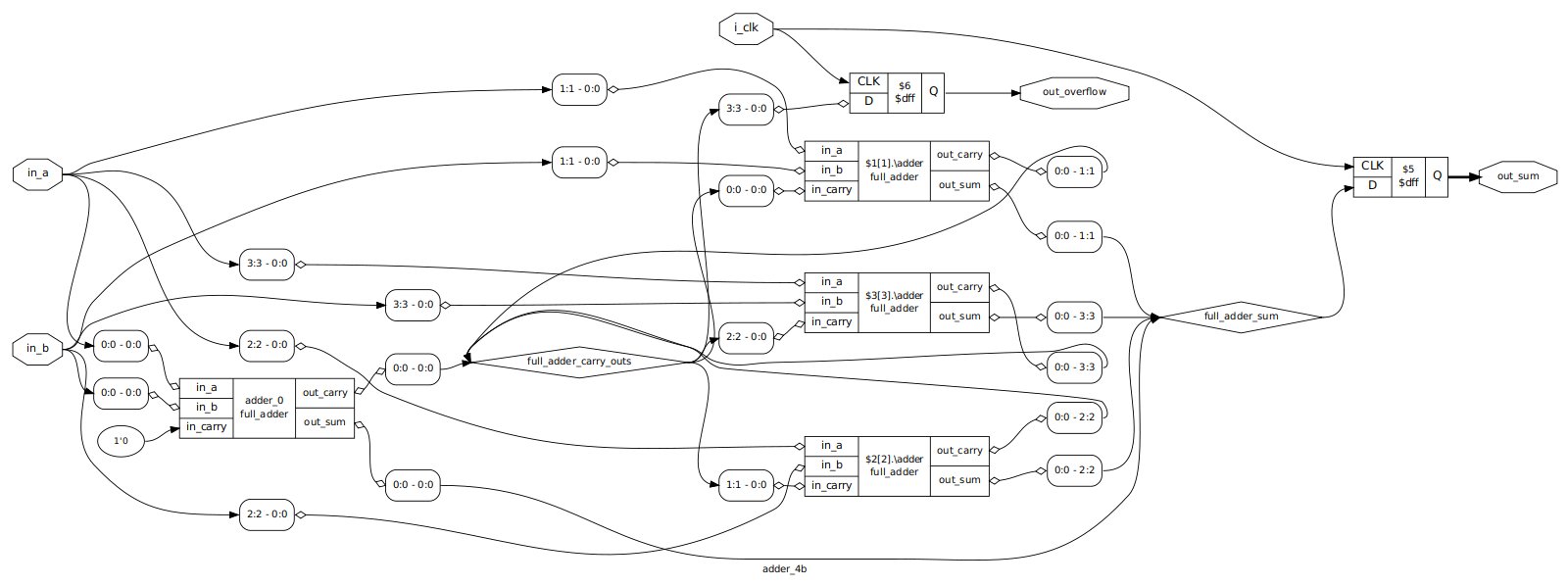
Clocked 4-Bit Adder
There is a lot more going on here! On the far left we can see our initial full
adder, with the zero’th bits of the input operands and a literal 0 bit as
inputs. The outputs then go off to the wire buses we defined, and we can see
the block of generated adder modules in the center. At the end, the final carry
bit goes to a D flip flop, which is clocked by our i_clk signal. Similarly,
the output sum data is fed to a 4-bit DFF that is also clocked.
Simulating with Verilator
In order to test and debug our HDL code, we could deploy it directly to a physical FPGA and hope for the best, but it can be much easier to first simulate parts or all of the design on the computer, allowing us to control and observe signals at a very low level, and to trace execution of the HDL over an arbitrary number of clock cycles. For Verilog, there exists an open source tool called Verilator that can take your Verilog source code and convert it to ordinary C code, which can then be linked against test benches of your own design. Let’s verify that our 4-bit adder works properly by creating a test bench that tests every possible combination of 4-bit values, and asserts that the result is correct.
First, we’re going to create a CMake based verilator setup (supported only on
more recent versions of verilator, I recommend at least 4.023). In our
CMakeLists.txt, let’s add the following:
cmake_minimum_required(VERSION 3.8)
project(four_bit_adder)

# We need to locate the verilator install path.
# If this doesn't work off the bat on your system, try setting
# the VERILATOR_ROOT environment variable to your install location.
# On a default install, this will be /usr/local/share/verilator
find_package(verilator HINTS $ENV{VERILATOR_ROOT} ${VERILATOR_ROOT})
if (NOT verilator_FOUND)
    message(FATAL_ERROR "Could not find Verilator. Install or set $VERILATOR_ROOT")
endif()

# Create our testbench executable.
# We will have just the one testbench source file.
add_executable(adder_testbench adder_testbench.cpp)

# Based on how I understand the verilator plugin to work, if you specify several
# verilog sources in the same target it will pick a top level module and
# only export the interface for that module. If you want to be able to poke
# around in lower-level modules, it seems that you need to specify them
# individually. To make this easier, I put all the sources in a list here
# so that I can add targets for them iteratively.
set(VERILOG_SOURCES
    ${PROJECT_SOURCE_DIR}/full_adder.v
    ${PROJECT_SOURCE_DIR}/adder_4b.v
)

# For each of the verilog sources defined above, create a verilate target
foreach(SOURCE ${VERILOG_SOURCES})
# We need to speicify an existing executable target to add the verilog sources
# and includes to. We also speicfy here that we want to build support
# for signal tracing
verilate(adder_testbench COVERAGE TRACE
    INCLUDE_DIRS "${PROJECT_SOURCE_DIR}"
    VERILATOR_ARGS -O2 -x-assign 0
    SOURCES ${SOURCE})
endforeach()
Now that we have a framework to build our testbench, let’s write something fairly straightforward in C. We will manually toggle the clock line while writing all our test inputs to the adder. We will then take the output and assert it matches what we calculate with C.
#include <stdlib.h>
#include <verilated.h>
#include <verilated_vcd_c.h>

#include <Vadder_4b.h>
#include <Vfull_adder.h>

int main(int argc, char **argv) {
  // Initialize Verilator
  Verilated::commandArgs(argc, argv);

  // Enable trace
  Verilated::traceEverOn(true);

  // Create our trace output
  VerilatedVcdC *vcd_trace = new VerilatedVcdC();

  // Create an instance of our module under test, in this case the 4-bit adder
  Vadder_4b *adder = new Vadder_4b();

  // Trace all of the adder signals for the duration of the run
  // 99 here is the maximum trace depth
  adder->trace(vcd_trace, 99);

  // Output the trace file
  vcd_trace->open("adder_testbench.vcd");

  // We need to keep track of what the time is for the trace file.
  // We will increment this every time we toggle the clock
  uint64_t trace_tick = 0;

  // For each possible 4-bit input a
  for (unsigned in_a = 0; in_a < (1 << 4); in_a++) {
    // For each possible 4-bit input b
    for (unsigned in_b = 0; in_b < (1 << 4); in_b++) {
      // Negative edge of the clock
      adder->i_clk = 0;
      // During the low clock period, set the input data for the adder
      adder->in_a = in_a;
      adder->in_b = in_b;
      // Evaluate any changes triggered by the falling edge
      // This includes the combinatorial logic in our design
      adder->eval();
      // Dump the current state of all signals to the trace file
      vcd_trace->dump(trace_tick++);

      // Positive edge of the clock
      adder->i_clk = 1;
      // Evaluate any changes triggered by the falling edge
      adder->eval();
      // Dump the current state of all signals to the trace file
      vcd_trace->dump(trace_tick++);

      // The adder should now have updated to show the new data on the output
      // buffer. Assert that the value and the overflow flag are correct.
      const unsigned expected = in_a + in_b;
      const unsigned expected_4bit = expected & 0b1111;
      const bool expected_carry = expected > 0b1111;
      // Check the sum is correct
      if (adder->out_sum != expected_4bit) {
        fprintf(stderr, "Bad result: %u + %u should be %u, got %u\n", in_a,
                in_b, expected, adder->out_sum);
        exit(EXIT_FAILURE);
      }
      // Check the carry is correct
      if (expected_carry != adder->out_overflow) {
        fprintf(stderr,
                "Bad result: %u + %u should set carry flag to %u, got %u\n",
                in_a, in_b, expected_carry, adder->out_overflow);
        exit(EXIT_FAILURE);
      }
    }
  }

  // Flush the trace data
  vcd_trace->flush();
  // Close the trace
  vcd_trace->close();
  // Testbench complete
  exit(EXIT_SUCCESS);
}
Now, if we build and run our testbench like so:
mkdir build
cd build
cmake ../
./adder_testbench
We should see… nothing! Our asserts should pass, and the testbench won’t
error out. We should also see that in the same directory from which we ran the
testbench, an adder_testbench.vcd file will have been created. This contains
the data of all the signals during our test case. We can open this file in
GTKWave or another wave viewer. If we click
on the TOP block in the SST tree, we should see the signals that are the
inputs and outputs to our four bit adder appear in the list view below.
Select all of them and hit ‘Append’ to place these signals on the scope view to
the right. Now you can scroll through time and observe that at the negative
edge of each clock, we set the new input data for the adder (this could also be
done at the posedge. At the following positive edge, we can see that the output
of the adder module correctly updates with the sum and overflow value.
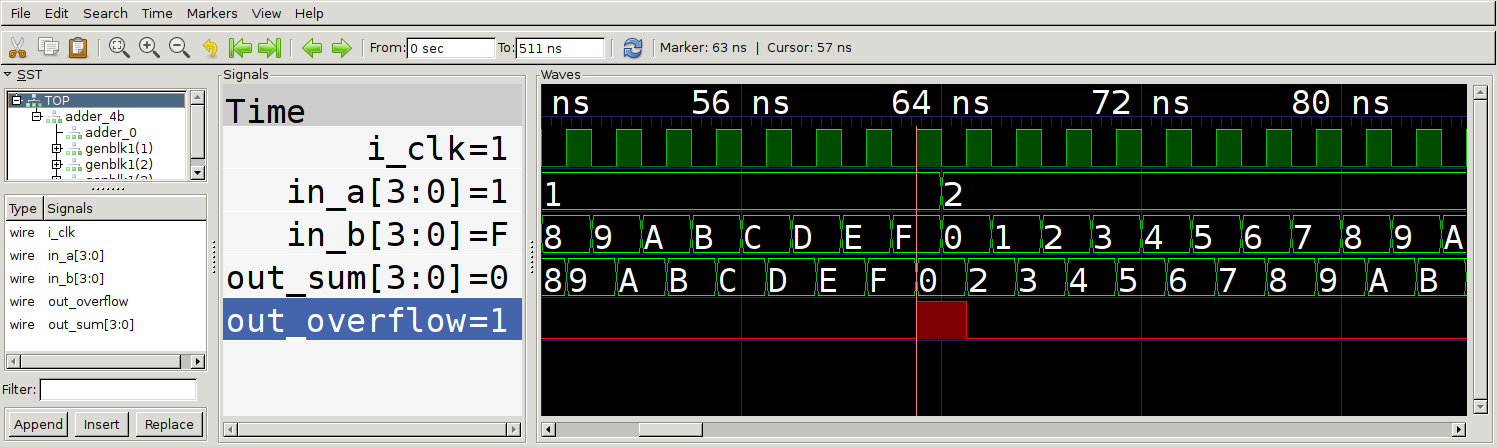
Trace output for our 4-bit adder testbench
Hopefully with this foundation, you feel comfortable writing, viewing the generated logic for and testing your own simple logic blocks. The full source code for the snippets listed in this post can be found on Github. If you have any corrections or improvements to suggest, feel free to do so.
In the next post, we create and deploy to an FPGA breakout board based on the Lattice Ice40 HX4k. After that, we use it to create an Animated GIF display on an LED panel and a RISC-V based SoC.